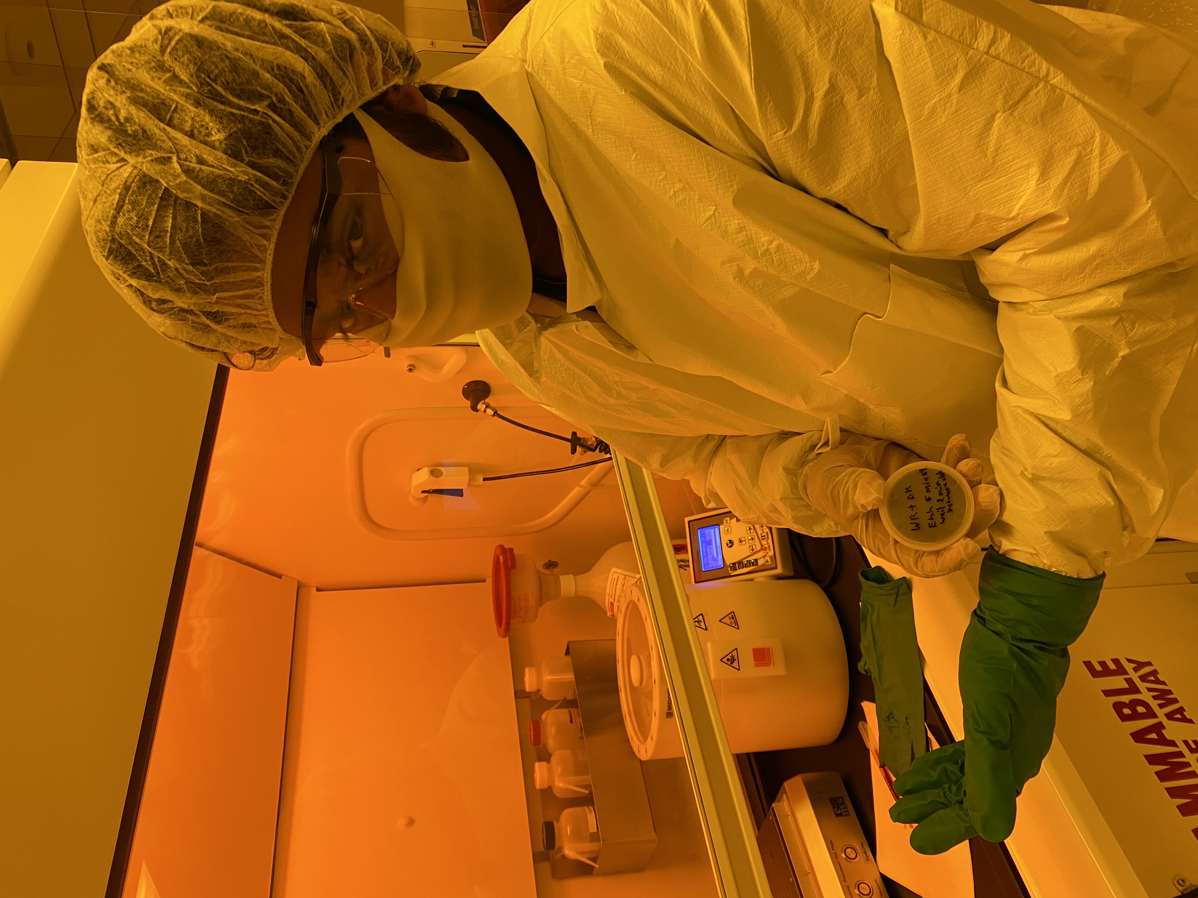
Semiconductor fabrication requires precise control over a sequence of physical and chemical processes, from lithography and thin-film deposition to etching and characterization. In this project, I worked through a multi-step integrated circuit fabrication workflow to gain hands-on experience with the methods used to manufacture and analyze semiconductor devices.
The project began with the design of a microlithography test mask. We used the mask to pattern structures on semiconductor wafers through photolithography, optimizing exposure and processing conditions to improve feature definition. Subsequent fabrication steps included wet etching, metal deposition, pattern liftoff, and device testing.
I also performed physical analysis of integrated circuits through de-encapsulation, cross-sectioning, and optical and electron microscopy. These measurements were used to examine device structure, estimate critical dimensions, identify back-end-of-line metal layers, and study features associated with the fabrication process.
Alongside the experimental work, I used TCAD software to simulate a PMOS fabrication process. This provided a complementary view of how individual processing steps affect device structure and helped connect the physical fabrication workflow with semiconductor process modeling.
The project provided experience across the semiconductor development cycle, including mask design, cleanroom processing, process optimization, microscopy, materials characterization, simulation, and interpretation of experimental results. It also reinforced the importance of understanding how individual fabrication steps interact to determine the performance and reliability of a completed semiconductor structure.